Chaintech 4SLE Motherboard - Part 2
6th July 2021
Welcome to Part 2 of my review of the Chaintech 4SLE Socket 3 VESA Local Bus motherboard! Here's that pic again:
So in Part 1 we took a look around this board from 1994 and established what its capabilities are. Mine is an early board revision, so we may find there are limitations. Over the years I have dug this board out and used it to test other PC hardware, and while it's very fiddly to get the configuration adjusted, when it's running it is rock solid - the main reason why I continue to use it for this purpose!
The Testing Setup
Aside from the Chaintech 4SLE motherboard, I will be using these additional items:
- A variety of CPUs, including Intel 486DX-33, 486DX2-66, and UMC U5-S-40
- Siemens-branded 8 MB double-sided 72-pin SIMM
- Various Super VGA VESA Local Bus graphics cards in addition to the odd CGA or EGA card ;-)
- Orpheus I sound card
The Jumpers
The Chaintech 4SLE is probably the worst motherboard in my collection when it comes to changing its configuration to work with different CPUs, memory, cache, etc. There are about 20 different jumpers to set and then double-check to be sure you're not about to blow anything up. In 1994 Socket 5 (Pentium) motherboards were largely becoming auto-configuring, something that could not come too soon for us PC hardware buffs!
Socket 3 boards have one serious drawback - there is no way for the socket to determine the level of voltage provided to it. The board has jumpers to set the socket's "Core Voltage" from 3.3V to 5V, and if this is incorrectly set I will instantly destroy the CPU. My motherboard here does not appear to have a voltage regulator fitted. You can see the big silver heatsink pad near the lower-left corner of the CPU socket - there should be a voltage regulator fitted there which has either been removed or [more likely] was never sold with one in the first place - I will be fitting a regulator here so I can test the board's operation with some of my 3.3V CPUs.
Initial Testing
But before I get ahead of myself, I want to dig into some of the BIOS settings:
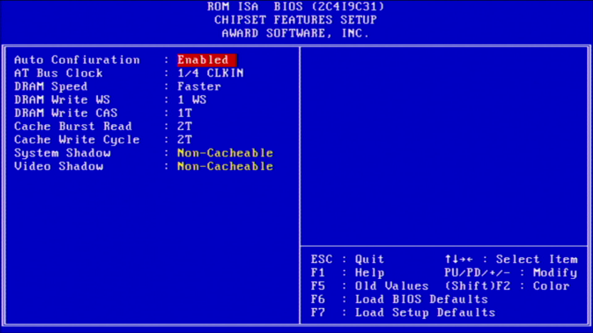
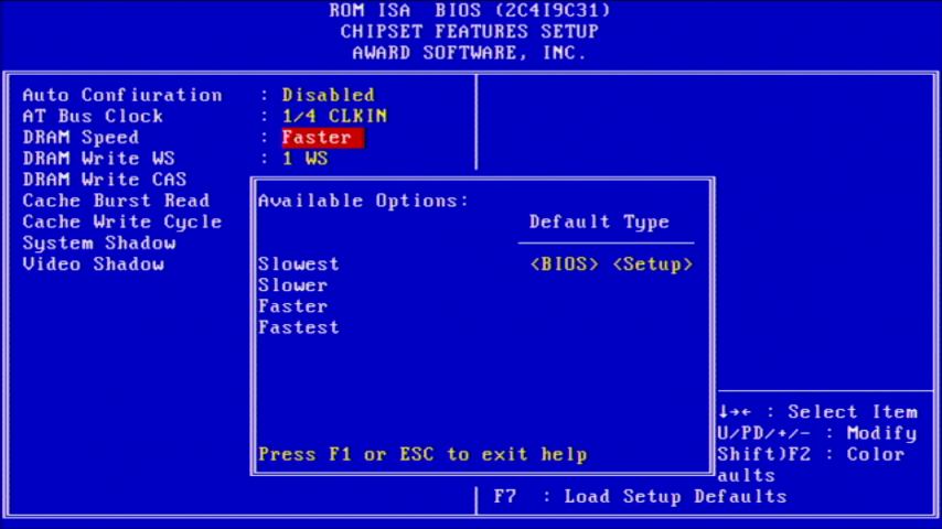
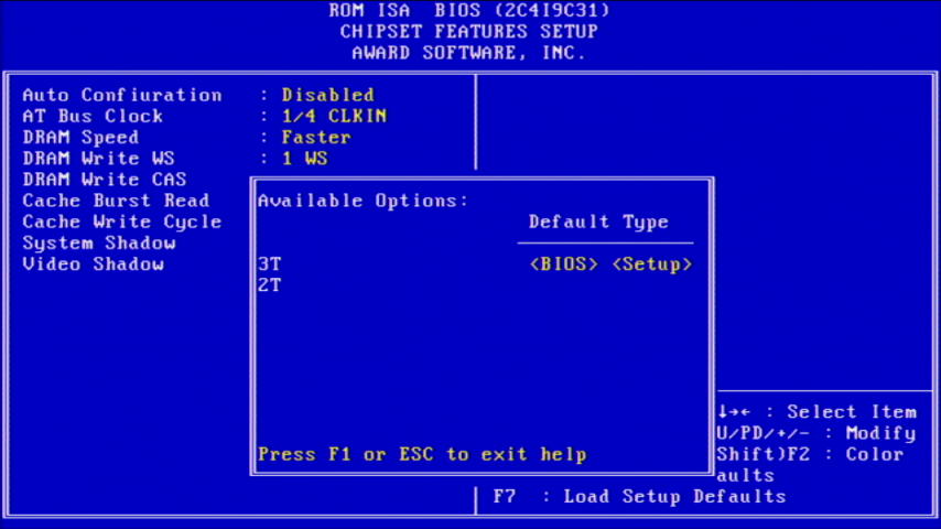
On the left above, the BIOS Features page is where you can enable or disable the L1 and L2 caches, set the 'Boot Up System Speed' from Low to High, and enable or disable ROM shadowing to RAM. On the right, the Chipset Features page is where you can alter the ISA bus speed, memory timings and enable or disable ROM shadow cacheing (I assume page 1's option simply copies BIOS ROM code to RAM whereas on page 2 it means those areas of RAM are then cacheable).
On this second page the available options are:
AT Bus Clock - the chipset generates a clock signal for the ISA bus. Its speed can either be fixed to 7.159 MHz or be set to a fraction of CLKIN (the CPU's frequency).
DRAM Speed - this allows you to select the access speed of the main memory according to the access time of the RAM you have installed. The faster the SIMMs you have installed, the higher you can set this.
DRAM Write WS - you can choose from 0 wait states on write operations to main memory, or 1 wait state.
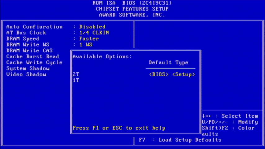
DRAM Write CAS - the number of clock cycles between sending a column address to the memory. Later referred to as CAS Latency, this is basically the time it takes for the memory to respond to the CPU when a write operation is requested.
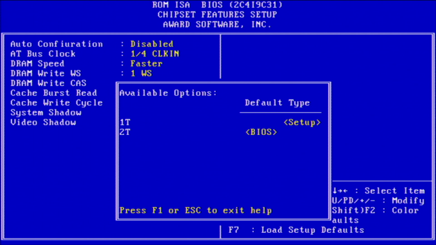
Cache Burst Read - the number of clock cycles it takes to read from the cache.
Cache Write Cycle - the number of clock cycles it takes to write to the cache.
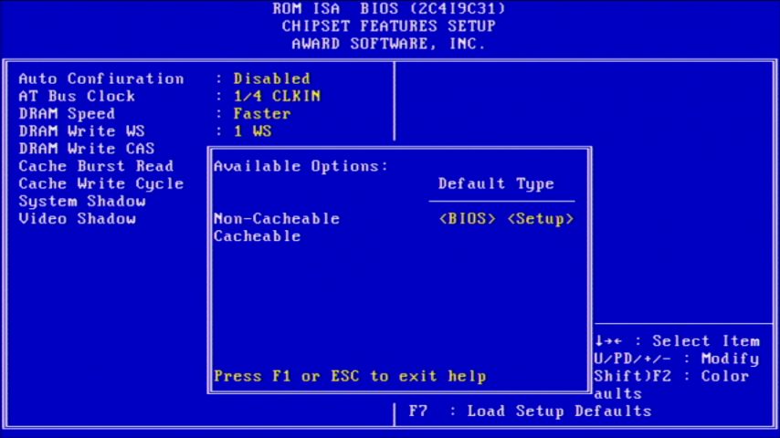
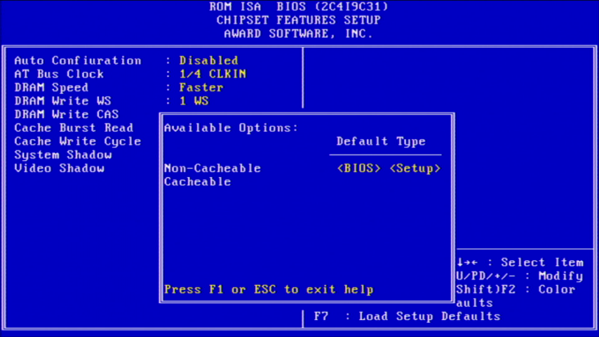
System Shadow - any ROM BIOS code that has been shadowed (copied to an area of RAM) can be set to cacheable or non-cacheable.
Video Shadow - the video card's ROM BIOS code that has been shadowed (copied to an area of RAM) can be set to cacheable or non-cacheable.
To keep track of what setting I am changing between tests, I will refer to my configurations by the settings I chose in the BIOS with a hyphen in between each, i.e. "[DRAM Speed] - [DRAM Write WS] - [DRAM Write CAS] - [Cache Burst Read] - [Cache Write Cycle]".
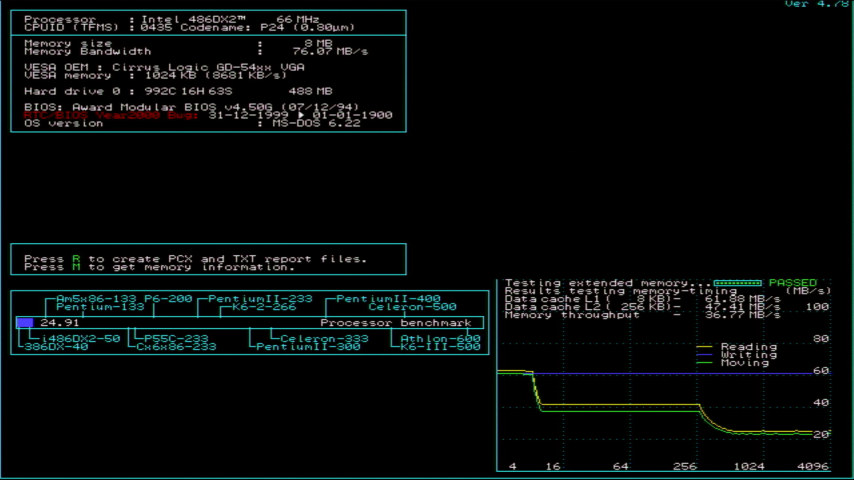
So running an Intel 486DX2-66 with the fastest possible settings of "Fastest-0-1-1-2" produced these memory performance timings:
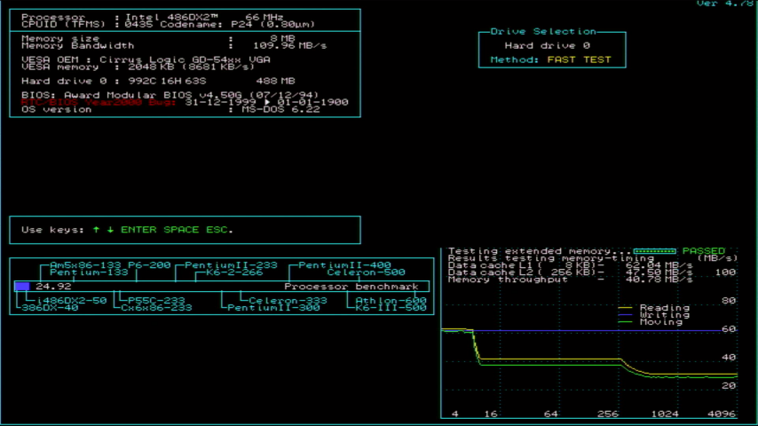
Changing the DRAM Speed from 'Fastest' to 'Faster' produced this:
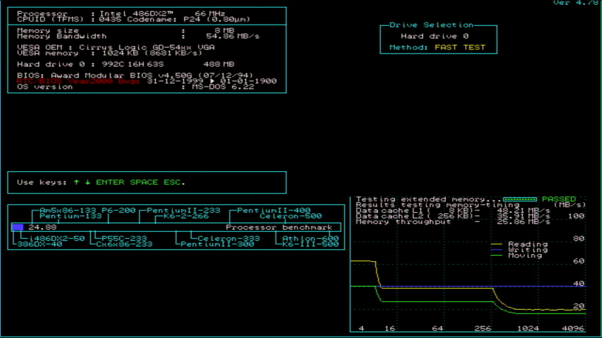
Changing the DRAM Speed to 'Slower' produced this:
And finally setting the DRAM Speed to 'Slowest':
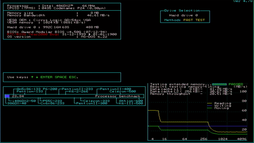
So there's a huge difference in memory throughput based on this one setting: DRAM Speed. Here's how it looks in tablular form:
| Slowest | Slower | Faster | Fastest | |
|---|---|---|---|---|
| L1 Cache | 41.25 | 48.21 | 61.88 | 62.04 |
| L2 Cache | 30.67 | 35.91 | 47.41 | 47.50 |
| Main Memory | 20.51 | 25.86 | 36.77 | 40.78 |
Now I will revert back to the 'Fastest' setting, but change each of the other memory timing BIOS settings to see what difference each makes. Let's start by setting the system to "Fastest-1-1-1-2", i.e. setting DRAM Write WS to 1:

You can see the memory performance has dropped by about 30% by adding this wait state.
Keeping the DRAM Write WS to zero but changing the DRAM Write CAS from 1T to 2T, i.e. a configuration of "Fastest-0-2-1-2" produced this:

So changing DRAM Write CAS from 1 to 2 T-states produced no drop in memory performance.
What about Cache Burst Read.... with a configuration of "Fastest-0-1-2-2" it failed to detect the L2 cache:

and last of all, setting the Cache Write Cycle from 2 T-states to 3 ("Fastest-0-1-1-3"):

As expected, the write performance has dropped (by about 30%), the same effect across the board as adding a wait state to DRAM Writes.
Here's the table showing all the figures together:
| Fastest-0-1-1-2 (BEST) |
Fastest-1-1-1-2 (1 DRAM Write WS) |
Fastest-0-2-1-2 (2T DRAM Write CAS) |
Fastest-0-1-2-2 (2T Cache Burst Read) |
Fastest-0-1-1-3 (3T Cache Write Cycle) |
|
|---|---|---|---|---|---|
| L1 Cache | 62.04 | 48.35 | 62.04 | 61.75 | 48.35 |
| L2 Cache | 47.50 | 37.62 | 47.50 | - | 37.62 |
| Main Memory | 40.78 | 32.03 | 40.78 | 40.78 | 32.03 |
Other Synthetic Performance Tests
For general synthetic performance tests, I ran the board using four sets of configuration settings, as follows:
Config 1 (Slowest):
BIOS boot speed set to low, Level 1 and 2 caches disabled, BIOS defaults for everything else.
Config 2 (Slow):
BIOS boot speed set to high, Level 1 and 2 caches enabled, all shadow RAM disabled, chipset timings on auto
Config 3 (Normal):
BIOS boot speed set to high, Level 1 and 2 caches enabled, all shadow RAM enabled, chipset timings on auto
Config 4 (Fastest):
BIOS boot speed set to high, Level 1 and 2 caches enabled, all shadow RAM enabled, fastest chipset timings
and ran these with some common synthetic DOS utilities against 3 of my Socket 3 CPUs:
- Intel 486DX (33 MHz)
- UMC U5-S (40 MHz)
- Intel 486DX2 (66 MHz)
Here were the results:
| DX-33 Cfg 1 |
U5S-40 Cfg 1 |
DX2-66 Cfg 1 |
DX-33 Cfg 2 |
U5S-40 Cfg 2 |
DX2-66 Cfg 2 |
DX-33 Cfg 3 |
U5S-40 Cfg 3 |
DX2-66 Cfg 3 |
DX-33 Cfg 4 |
U5S-40 Cfg 4 |
DX2-66 Cfg 4 |
|
|---|---|---|---|---|---|---|---|---|---|---|---|---|
| SpeedSys v4.78 | 7.52 | 24.80 | 24.79 | 24.92 | ||||||||
| Norton SI 4.50 | 28.2 | 9.4 | 21.1 | 52.1 | 106.3 | 109.6 | 52.1 | 100.7 | 104.0 | 52.2 | 101.8 | 110.5 |
| Norton SI 8.0 | 27.8 | 4.3 | 9.5 | 71.0 | 90.5 | 125.3 | 71.0 | 90.5 | 124.7 | 71.0 | 107.5 | 142.5 |
| AGSI Dhrystones | 6574 | 1116 | 2656 | 14829 | 22585 | 27421 | 14841 | 22561 | 27296 | 15259 | 26484 | 30187 |
| AGSI KWhetstones | 3100 | 19 | 1634 | 4958 | 353 | 9944 | 4979 | 353 | 9659 | 5000 | 380 | 10150 |
| NSSI | 8959 | 4017 | 5321 | 17139 | 23797 | 29000 | 18077 | 23664 | 29000 | 18138 | 26756 | 31448 |
| CacheChk L1 (MB/s) | - | - | - | 83.6 | 83.7 | 67.9 | - | 83.7 | 67.9 | 34.4 | 83.8 | 68.6 |
| CacheChk L2 (MB/s) | - | - | - | 38.5 | 47.8 | 37.1 | 29.2 | 47.8 | 37;1 | - | 51.6 | 46.3 |
| CacheChk Main Memory (MB/s) | 5.8 | 6.3 | 18.8 | 24.9 | 22.2 | 26.7 | 16.7 | 22.2 | 26.7 | 22.5 | 37.1 | 33.3 |
| Dr.Hard Hardstones | 6492 | 1406 | 2601 | 15137 | 21722 | 27910 | 15134 | 21722 | 27929 | 16453 | 24261 | 30478 |
| Dr.Hard Softstones | 3975 | 34 | 2133 | 6625 | 662 | 13117 | 6625 | 662 | 13117 | 6625 | 681 | 13117 |
| Dr.Hard RAM max (MB/s) | 7.43 | 3.03 | 8.60 | 24.43 | 26.70 | 40.39 | 24.43 | 26.70 | 40.72 | 37.59 | 40.72 | 61.09 |
| Dr.Hard RAM std(MB/s) | 5.62 | 2.05 | 4.84 | 17.80 | 20.43 | 22.76 | 17.82 | 20.43 | 22.84 | 21.79 | 30.26 | 33.19 |
| Dr.Hard RAM min(MB/s) | 3.99 | 1.65 | 3.82 | 12.82 | 15.33 | 17.95 | 12.95 | 15.28 | 17.95 | 15.04 | 23.13 | 24.97 |
Of course, the 486DX2-66 is the powerhouse here, but it should be noted just how good the UMC U5-S microprocessor really is. Ignoring the KWhetstones tests above (being an "SX" chip it doesn't have a built-in math coprocessor), the expectation is that it would be about 21% faster than the 486DX-33, and about 40% slower than the 486DX2-66. The reality is that it's anywhere from 47% to 70% faster than the 486DX-33, and between 11% and 23% slower than the 486DX2-66. It also returned the best CacheChk results of all 3 CPUs on the Chaintech 4SLE motherboard.
Real World Performance Tests
For gaming, I set the board to its fastest possible BIOS settings that were identified above. The motherboard has two VESA Local Bus jumpers: JP15 selects between "<=33 MHz" and ">33 MHz", and JP16 selects "0 WS" or "1 WS". Adjusting these made no difference to the real-world performance benchmarks:
With a 486DX/2-66 CPU set to the fastest possible settings in the BIOS and AT BUS Clock set to 1/2 CLKIN, I ran Phil's Computer Lab's collated set of DOSBench utilities using several graphics cards:
| EliteGroup VI-711A CL-GD5428 1 MB 60ns VLB |
Orchid Fahrenheit VA/VLB S3 86C805 1 MB 60/70ns VLB |
(Unknown Brand) CL-GD5424 512 KB |
(Unknown Brand) WD90C30-LR 512 KB 70ns ISA |
|
|---|---|---|---|---|
| 3DBench 1.0c | 45.3 | 47.7 | 37.3 | |
| Chris 3D Benchmark | 29.5 | 29.5 | 24.2 | |
| Chris 3D Benchmark 640x480 | 8.9 | 7.3 | 7.3 | |
| PC Player (320x200x8bpp) | 11.3 | 11.3 | 10.5 | |
| PC Player (640x480x8bpp) | 4.6 | 4.6 | 4.0 | |
| Doom timedemo (max. details) | 26.8 (2782 RT, 2134 GT) | 28.6 (2610 RT, 2134 GT) | 21.0 (3549 RT, 2134 GT) | |
| Quake timedemo | 7.8 | 7.8 | 7.5 | |
| Quake timedemo (640x480) | 6.7 | 7.8 | 7.4 |
The EliteGroup card has a jumper to switch between its onboard 14 MHz clock or use the ISA bus clock. Changing this made no difference to the benchmark results.
In Part 3, I will look to getting that voltage regulator fitted so we can push this mobo to the max with a few of my later Socket 3 CPUs.


